经过生产验证的,复杂的半导体IP核

半导体电路设计IP及配套交付件


T2M LVDS / FPD link Tx IP

LVDS / FPD link Tx IP

概述和功能介绍

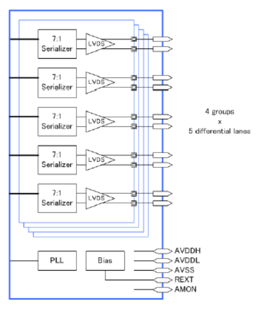
A physical layer IP for LVDS transmitter. This IP consists of 20-lane (4 x 4D1C) LVDS drivers, and supports up to 1.5Gbps data rate.In LVDS mode, both the serial and parallel data are organized into 4 channels. The parallel data is 7 bits wide per channel. The input clock is 25MHz to 150MHz. The serializer is highly integrated and requires no external components. The circuit is designed in a modular fashion and desensitized to process variations. This facilitates process migration, and results in a robust design.


功能描述
  • LVDS compliant Tx
  • 4 groups of 4-Data
  • 1-Clock channels Each lane/group can be turned on/off individually Data/Clock can be assigned to any lane within the group
  • Differential polarity can be flip per lane
  • Supports from 168Mbps to 1.5Gbps data rate
  • Supports reduced swing mode
  • X7 Multiplier PLL for serial clock generation
  • Configurable analog characteristics
  • PLL loop filter
  • PLL VCO gain
  • Differential voltage Common-mode voltage
  • Pre-emphasis strength

Deliverables

  • Datasheet
  • Integration guideline
  • GDSII or Phantom
  • GDSII Layer map table
  • CDL netlist for LVS
  • LEF Verilog behavior model
  • Liberty timing model DRC/LVS/ERC results
Benefits
  • Testability
  • At speed test by Loopback BIST
  • Internal analog nodes can be observed through a test pad
  • Supports VCO gain test, transmitter DC test, IDDQ test
Applications
  • Smart Phone
  • Tablet
  • PC
  • Car navigation
  • Smart TV
  • Digital Still Camera
  • HD Camera