经过生产验证的,复杂的半导体IP核

半导体电路设计IP及配套交付件


T2M V-by-One / LVDS Rx IP

V-by-One / LVDS Rx IP

概述和功能介绍

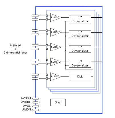
V-by-One® HS technology targets a high speed data transmission of video signals based on internal connection of equipment. V-by-One® HS Standard defines the specifications to develop a transmitter and receiver .This Supports up to 4Gbps/lane; and Available 8-lane PHY and 16-lane PHY for Tx and Rx. A physical layer IP for LVDS Receiver. This IP consists of 20-lane (4 x 4D1C) LVDS receivers, and supports up to 1.5Gbps data rate. The input clock is 25MHz to 150MHz. The serializer is highly integrated and requires no external components. The circuit is designed in a modular fashion and desensitized to process variations. This facilitates process migration, and results in a robust design.

 V-by-one-LVDS-Rx-IP-supplier-in-china 

功能描述
  • LVDS compliant Rx
  • 4 groups of 4-Data, 1-Clock channels
  • Each lane/group can be turned on/off individually
  • Supports from 168Mbps to 1.5Gbps data rate
  • Configurable analog characteristics
  • Bias voltage/current
  • DLL characteristics
  • Testability Internal analog nodes can be observed through a test pad DLL test mode Process
  • Testability At speed test by Loopback BIST
  • Internal analog nodes can be observed through a test pad
  • Supports VCO gain test, transmitter DC test, IDDQ test
  • Supply Voltage 1.8V/0.9V

Deliverables

  • Datasheet
  • Integration Guideline
  • GDS or Phantom GDS
  • Layer Map Table
  • CDL Netlist for LVS
  • LEF
  • Verilog Behavior Model
  • Liberty Timing Model
  • DRC/LVS/ERC results
  • RTL for Digital section
  • Test Spec Document

Applications

  • Smart Phone
  • Tablet
  • PC
  • Car navigation
  • Smart TV
  • Digital Still Camera
  • HD Camera