The full gamut of PCIe 2.0 Base operations is covered by PCIe 2.0 transceiver IP. It conforms to the PIPE 3.0 standard. This IP combines high-speed mixed signal circuits to handle PCIe 2.0 traffic at 5Gbps and is backward compatible with PCIe 1.0 data rate at 2.5Gbps. It is intended to consume less power and have a small die area. The requirements for various channel conditions can be fulfilled by the PCIe 2.0 IP owing to its support for both TX and RX equalisation techniques.
Compatible with PCIe base Specification
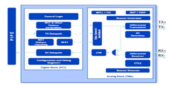
Full compatible with PIPE3.0 interface specification
Independent channel power down control
Implemented Receiver equalization Adaptive-CTLE to compensate insertion loss
Support 16-bit/32bit parallel interface
Support for PCIe gen1(2.5Gbps) and PCIe gen2(5.0Gbps)
Support flexible reference clock frequency
Support 100MHz differential reference clock input or output (with SSC optionally) in PCIe Mode
Support Spread-Spectrum clock (SSC) generation and receiving from -5000ppm to 0ppm
Support programmable transmit amplitude and Deemphasis
Support TX detect RX function in PCIe Mode
Support Beacon signal generation and detection in
Production test support is optimized through high coverage at-speed BIST and loopback
Integrated on-die termination resistors and IO Pads/Bumps
Embedded Primary & Secondary ESD Protection
ESD: HBM/MM/CDM/Latch Up 2000V/200V/500V/100mA
Silicon Proven in TSMC 40nm LP
Deliverables
GDSII & layer map
Place-Route views (.LEF)
Liberty library (.lib)
Verilog behaviour model
Netlist & SDF timing
Layout guidelines, application notes
LVS/DRC verification reports
